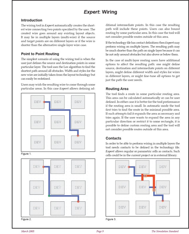
Expert Parametric Wires

Expert Parametric Wire (Pwire) is a complex group of objects containing, a single wire named master wire, any number of subparts such as enclosure wires, offset wires and sets of rectangles. Pwire objects enable extremely quick and efficient creation and editing of guard rings and shielded paths which are increasingly important due to higher integration density of IC designs.
Continue ReadingExpert Parametric Wires

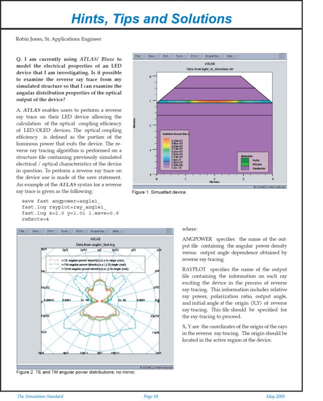
I am currently using ATLAS/ Blaze to model the electrical properties of an LED device

I am currently using ATLAS/ Blaze to model the electrical properties of an LED device that I am investigating. Is it possible to examine the reverse ray trace from my simulated structure so that I can examine the angular distribution properties of the optical output of the device?

Continue ReadingI am currently using ATLAS/ Blaze to model the electrical properties of an LED device

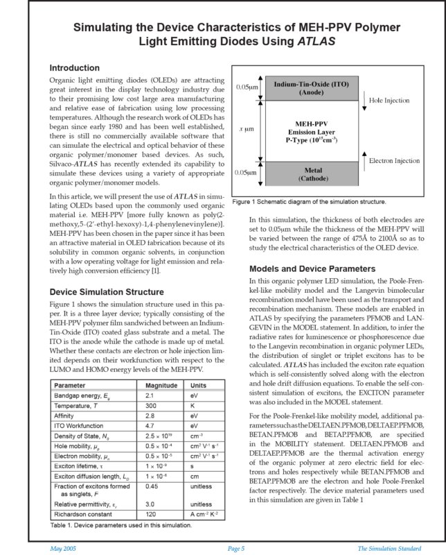
Simulating the Device Characteristics of MEH-PPV Polymer Light Emitting Diodes Using Atlas

Organic light emitting diodes (OLEDs) are attracting great interest in the display technology industry due to their promising low cost large area manufacturing and relative ease of fabrication using low processing temperatures. Although the research work of OLEDs has began since early 1980 and has been well established, there is still no commercially available software that can simulate the electrical and optical behavior of these organic polymer/monomer based devices. As such, Silvaco-ATLAS has recently extended its capability to simulate these devices using a variety of appropriate organic polymer/monomer models.

Continue ReadingSimulating the Device Characteristics of MEH-PPV Polymer Light Emitting Diodes Using Atlas

A Comprehensive Solution for Simulating Ultra-Shallow Junctions: From High Dose/Low Energy Implant to Diffusion Annealing

The persistent semiconductor technology trend of shrinking down device size requires development of veryaggressive technological setups consisting in high dose/low energy implants, followed by rapid thermal anneals (RTA).

Continue ReadingA Comprehensive Solution for Simulating Ultra-Shallow Junctions: From High Dose/Low Energy Implant to Diffusion Annealing

Expert: Wiring

The wiring tool in Expert automatically creates the shortest wire connecting two points specified by the user. The created wire goes around any existing layout objects. It may lie in multiple layers (multi-wire) if the source and target points are on different layers or if the wire is shorter than the alternative single-layer wire case.

Continue ReadingExpert: Wiring

New Parasitic Capacitance Modeling in Hipex-C

In deep submicron technology, conduction layers have widths much smaller than their thicknesses (see Figure 1). This makes edge parasitic capacitance effects more dominant than plate capacitance. In a multi-body system, neighboring conductors may capture some or all of the electrical fields lines emanating from a particular conductor. These field lines would otherwise terminate else where. This phenomenon is called charge sharing, which plays an important role in modeling parasitic capacitances.

Continue ReadingNew Parasitic Capacitance Modeling in Hipex-C

Capacitance Coupling Calculation of IPS mode TFT-LCD Using Clever

The increasing demand of the TFT-LCD industry has lead to a rapid growth in display size and resolution. The higher cell packing density results in a narrowing viewing angle and image degradation due to electrical coupling between the data bus lines and display electrodes. This “crosstalk” therefore becomes a serious limitation. The in-plane switching(IPS) mode has been used as an excellent technology solution for realizing extremely wide viewing angles.

Continue ReadingCapacitance Coupling Calculation of IPS mode TFT-LCD Using Clever